INFORMATION
Description
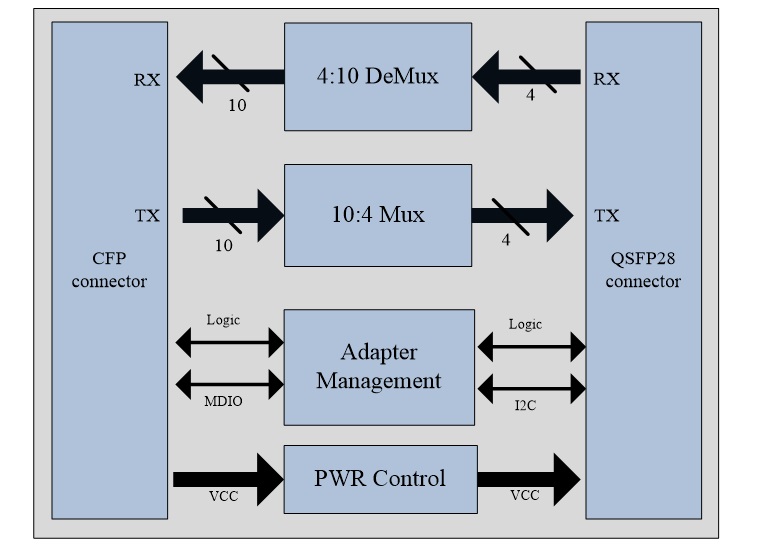
The 100G CFP to QSFP28 Adapter module is a
high performance, hot pluggable, and interconnect solution supporting 100G
Ethernet and Telecom. The Adapter converts a CFP MSA interface to 1-port of
100GE QSFP28.It is compliant with the CFP MSA. Baudcom100G CFP to QSFP28 Adapter
module converts 10 bidirectional 10G channels to 4 bidirectional 25G channels
operating at up to 28Gbps per channel. The Adapter supports FEC (Forward Error
Correction) function; the user can enable the FEC function through the register
configuration.
As shown in Figure 1, the transmitter side
of the adapter converts 10 parallel electrical data inputs to 4parallel electrical
data output signals through a 10:4 multiplexing and associated circuitry. The receiver
side of the adapter converts 4 parallel electrical signals into 10 parallel
electrical signals through a 4:10 De multiplexing and associated circuitry.
Features
Compliant
to CFP Hardware Specification Version 1.4
Compliant to CFP MSA Management Interface
Specification Version 2.2
Converts 10 bidirectional 10G lanes to4
bidirectional 25G lanes
1 port QSFP28 TX&RX
Support 100G IEEE 802.3bj NRZ FEC
Transmission data rate up to 28Gbps per
channel
OTU4 compatible(FEC is invalid
when OTU4 data rate mode is on)
FEC is configurable
MDIO digital diagnostic interface and control
capabilities
Power class 2 (Adapter<5W max)
Hot pluggable electrical interface
Operating case temperature:0°C~ +70°C
Single 3.3V power supply
RoHS 6 compliant(lead free)
Applications
100GBE interconnects, IEEE 802.3ba 100GBASE-LR4(Adapter+QSFP28_LR4), IEEE
802.3bm 100GBASE-SR4(Adapter+QSFP28_SR4)
High-speed core router connections& Datacom/Telecom switch
Data aggregation and backplane applications
Proprietary protocol and density application
Specification
Absolute Maximum Ratings
|
Parameter
|
Symbol
|
Min
|
Max
|
Unit
|
|
Supply Voltage
|
Vcc
|
-0.5
|
3.6
|
V
|
|
Input Voltage
|
Vin
|
-0.3
|
Vcc+0.3
|
V
|
|
Storage Temperature
|
Tst
|
-20
|
85
|
oC
|
|
Humidity(non-condensing)
|
Rh
|
5
|
85
|
%
|
*Exceeding
any one of these values may destroy the device immediately
Recommended Operating Conditions
|
Parameter
|
Symbol
|
Min
|
Typical
|
Max
|
Unit
|
|
Supply Voltage
|
Vcc
|
3.13
|
3.3
|
3.47
|
V
|
|
Operating Case temperature
|
Tca
|
0
|
|
70
|
oC
|
|
Data RatePer Lane
|
10GBE
|
fd
|
-
|
10.3125
|
11.2
|
Gbps
|
|
25GBE
|
25.78125
|
27.952
|
|
Power Dissipation
|
Pm
|
|
|
5
|
W
|
|
Low Power Mode Dissipation
|
Plow
|
|
|
2
|
W
|
|
Aggregate Bit Rate
|
BRaggr
|
|
103.125
|
111.8
|
Gbps
|
Electrical Characteristics
|
Parameter
|
Symbol
|
Min
|
Typical
|
Max
|
Unit
|
Notes
|
|
Differential input
impedance
|
Zin
|
90
|
100
|
110
|
ohm
|
|
|
Differential Output
impedance
|
Zout
|
90
|
100
|
110
|
ohm
|
|
|
10GBE
|
Differential input voltage amplitude
|
ΔVin
|
120
|
|
820
|
mVp-p
|
1
|
|
Differential output voltage amplitude
|
ΔVout
|
300
|
|
820
|
mVp-p
|
2
|
|
25GBE
|
Differential input voltage amplitude
|
ΔVin
|
300
|
|
1100
|
mVp-p
|
1
|
|
Differential output voltage amplitude
|
ΔVout
|
500
|
|
900
|
mVp-p
|
2
|
|
Bit Error Rate
|
BER
|
|
|
E-12
|
|
3
|
|
Input Logic Level High
|
VIH
|
2.0
|
|
VCC+0.3
|
V
|
3.3V LVCOMS
|
|
0.84
|
|
1.5
|
V
|
1.2V LVCOMS
|
|
Input Logic Level Low
|
VIL
|
-0.3
|
|
0.8
|
V
|
3.3V LVCOMS
|
|
-0.3
|
|
0.36
|
V
|
1.2V LVCOMS
|
|
Output Logic Level
High
|
VOH
|
VCC-0.2
|
|
VCC
|
V
|
3.3V LVCOMS
|
|
1.0
|
|
1.5
|
V
|
1.2V LVCOMS
|
|
Output Logic Level Low
|
VOL
|
0
|
|
0.2
|
V
|
3.3V LVCOMS
|
|
-0.3
|
|
0.2
|
V
|
1.2V LVCOMS
|
Note:
1. Differential
input voltage amplitude is measured between
TxnP and TxnN.
2. Differential
output voltage amplitude is measured between
RxnPand RxnN.
3.
BER=10^-12; PRBS 2^[email protected]/25.78125Gbps.
Reference Clock Characteristics
|
Parameter
|
Symbol
|
Min
|
Typical
|
Max
|
Unit
|
Notes
|
|
Impedance
|
Zd
|
80
|
100
|
120
|
Ω
|
|
|
Frequency
|
|
|
161.1328125
/644.53125
|
174.7030837
/698.8123348
|
MHz
|
1/64 or 1/16 ofelectrical lane rate
|
|
FrequencyStability
|
△f
|
-100
|
|
100
|
ppm
|
For Ethernetapplications
|
|
-20
|
|
20
|
For Telecomapplications
|
|
OutputDifferentialVoltage
|
VDIFF
|
400
|
|
1200
|
mV
|
Peak to
PeakDifferential
|
|
RMS jitter
|
σ
|
|
|
10
|
ps
|
Random
Jitter. Overfrequency band of10KHz<f<10MHz
|
|
Clock DutyCycle
|
|
40
|
|
60
|
%
|
|
|
ClockRise/FallTime10%/90%
|
tr/f
|
200
|
|
1250
|
ps
|
1/64 of
electrical lane rate
|
|
50
|
|
315
|
1/16 of
electrical lane rate
|
FEC control register
|
Address
|
AccessType
|
BitWidth
|
|
Description
|
Notes
|
|
0x91FC
|
R/W
|
1
|
|
0x0:Enable FEC.
0x1:Disable FEC.
|
FEC is invalid when OTU4 data rate mode is on
|
FEC control register 0x91FC supports reconfiguration and save function:
1. Write value to 0x91FC;
2. Read the address 0xA004 = 0000h(Idle);
3. Save command, writes value 0001h to address 0x91F0;
4. Read status, wait until the address 0xA004 = 0004h(save success), and then read the address again 0xA004 = 0000h(Idle, read twice to ensure status is cleared).
Normally saving needs about 1 second, but the longest time is about 4
seconds, we suggest customer can read 0xA004 after waiting for a while.
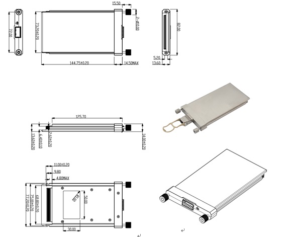
Mechanical Dimensions
Important Notice
Performance figures, data and any illustrative material
provided in this data sheet are typical and must be
specifically confirmed in writing by Baudcom before
they become applicable to any particular order or contract. In accordance with
the Baudcom policy of continuous improvement specifications may change without notice.
The publication of information in this data sheet does
not imply freedom from patent or other protective rights of Baudcom or
others. Further details are available from any Baudcom sales representative.
Ordering information
Related Products
